Posts

Showing posts from October, 2021

VLSI (PROPAGATION DELAY)

Image
 PROPAGATION DELAY: The time required for charging/discharging to change the output from logic 0 to logic 1 or vice versa is called propagation delay. propagation delay(Tpd) should be as low as possible to get fast switching speeds. CMOS is a single RC network and propagation delay of such circuit if excited by V step voltage is :                              tphl = ln(2) Reqn CL = 0.69 Req CL                              tplh = ln(2) Reqp CL = 0. 69 Req CL the total propagation delay is                                tp=(tphl+tplh)/2 = 0. 69(Reqn + Reqp)/2 propagation delay can be reduced in the following ways: Reduced CL : careful design of CMOS reduces diffusion and interconnection capacitances. Increase in W with cons...

VLSI (NOISE MARGIN)

Image
 NOISE MARGIN: it is defined as up to what extent noise is allowed so that there is proper extraction of logic 1 and logic 0. NMh is the noise margin for logic high. NMl is the noise margin for logic low. this above noise margin explains that even if you connect the output of the circuit to another circuit at the input that much noise is allowed(NMh, NMl). the gap between Vih and 

VLSI (STATIC POWER CONSUMPTION IN CMOS)

Image
 STATIC POWER CONSUMPTION IN CMOS: The current that flows between the power rails when there is no switching activity i.e, there is no switching taking place from 0--->1 or 1---->0 at the input it is more like a steady-state. There is, unfortunately, a leakage current flowing through the reverse-biased diode junctions of the transistors, located between the source or drain and the substrate.  This contribution is, in general, very small and can be ignored. however this leakage current is increased by temperature. Their value increases with increasing junction temperature, and this occurs in an exponential fashion.

VLSI (CMOS INVERTER)

Image
 CMOS INVERTER:

VLSI (LOGIC STYLE CLASSIFICATION)

Image
 

VLSI (MOSFET CAPACITANCES)

Image
 MOSFET CAPACITANCES: speed of the integrated circuit is limited by capacitance so that is why we should study this topic. here we will know the capacitances present in the MOSFET i.e., distributed capacitances( capacitance formed at lower frequency). MOS CAPACITANCES AT DIFFERENT REGIONS:

VLSI (STATIC POWER DISSIPATION)

 STATIC POWER DISSIPATION: Assume there is a circuit that consists of a number of MOSFETs. let's take one of the transistors from that circuit, here if Vgs<Vth the transistor is supposed to be OFF. But there is some leakage current that is flowing resulting in a power dissipation. so, when the circuit is in IDLE state or OFF state there is currently flowing through and there is some power dissipation. This Power dissipation which is occurring is called STATIC POWER DISSIPATION.

VLSI (SUBTHRESHOLD CONDITION)

Image
 SUBTHRESHOLD CONDITION: when Vgs>Vth, we know that current will flow through the MOSFET. when Vgs < Vth, the current that flows through the MOSFET should be '0'. But there is a small negligible current that is flowing through the MOSFET. This current which is flowing through MOSFET when Vgs < Vth is called SUBTHRESHOLD CONDITION. when Vgs goes less than Vth the current isn't abruptly dropping down to 0 rather the current is exponentially decreasing which is observing by the below equation.  the subthreshold current leads to static power dissipation. the subthreshold current equation is:                    Ids = Idso * e^[(Vgs-Vth)/nVt] * [1-e^(-Vds/Vt)]                                   Idso=beta * Vt^2 * e^1.8 Idso is current at threshold voltage depends on process and device geometry. n is non ideality factor(n...

VLSI (FABRICATION PROCESS OF NMOS)

Image
 FABRICATION OF NMOS: step 1: processing starts on single-crystal silicon of high purity on which required p impurities are introduced as the crystal is grown. such wafers are about 75 to 150mm in diameter and 0.4 mm thick. step 2: A layer of silicon dioxide (SiO2) typically 1 micrometer thick is grown all over the surface of the wafer to protect the surface, acts as a barrier to the dopant during processing, and provide a generally insulating substrate. step 3: the surface is covered with photo resistance which is evenly distributed over the surface. step 4: the photo resistant layer is exposed to ultraviolet rays through masking which defines the region which diffusion is to takes place together with transistor channels. step 5: these areas are readily etched away together with the underlying silion dioxide layer. step six: the remaining photoresist is removed and a thin layer of the oxide layer is deposited over the total surface. step 7: after depositing the...

DSP (LIMITATIONS OF PIPELINING IN DSP)

 LIMITATIONS OF PIPELINING: The design of a non-pipelined processor is simpler and cheaper to manufacture.  Non-pipelined processor executes only a single instruction at a time. This prevents branch delays (in Pipelining, every branch is delayed) as well as problems when serial instructions being executed concurrently. In pipelined processor, insertion of flip flops between modules increases the instruction latency compared to a non-pipelining processor. A non-pipelined processor will have a defined instruction throughput. The performance of a pipelined processor is much harder to predict and may vary widely for different progams. When a programmer (or compiler) writes assembly code, they generally assume that each instruction is executed before the next instruction is being executed. When this assumption is not validated by pipelining it causes a program to behave incorrectly, the situation is known as a hazard. Unfortunately, not all instructions are independent. In a simple...

DSP (CHARACTERISTICS OF WINDOW)

 CHARACTERISTICS OF WINDOW: MAIN LOBE WIDTH : The measure of the main lobe width at -3dB or -6dB below the main lobe peak. When the main lobe width decreases, the remaining energy spreads out to the side lobes and thereby decreasing the detection ability. A compromise is needed to find the balance between detection and resolution fitting for a given application. SIDE LOBES : Side lobes occur at either side of the main lobe. They approach zero at integral multiples of Fs/N where Fs=sampling frequency and N is the length of N-point FFT/DFT. Side lobes directly affect the extent to which the adjacent frequency components leak into the adjacent frequency bins. SIDE LOBE HEIGHT  : The side lobe height is usually measured for the side lobe with the maximum peak compared to other side lobes. It is measured in decibels relative to the peak of the main lobe. SIDE LOBE ROLL-OFF RATE  : The asymptotic decay rate in decibels per decade of the frequency of the side lobes’ peaks. EQUIV...

DSP (MUTLIRATE SIGNAL PROCESSING)

 MULTI RATE SIGNAL PROCESSING: Multi rate signal processing  which includes sample rate conversion. Enables processing of different type of signals with different sample rates. Reduce the need for expensive anti-aliasing filters. can improves the flexibility of software studio. Wideband receivers make use of multi rate signal processing for efficient channelization.  

VLSI (CMOS LATCH UP)

Image
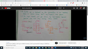
 LATCH UP IN CMOS: what is meant by latch-up? Generation of low impedance patch between the Vdd and GND in CMOS circuit. This makes a high amount of current driven from Vdd to GND by this the CMOS will be destroyed. SCR analogy to understand the latch-up: let us take four-layer SCR like below and apply Vdd at the anode and GND at the cathode. after you are given the Vdd and GND, if we give a trigger( small pulse) at the gate the SCR will Turn ON now current flows through it but there is no chance to turn it Off, This is called latch-up in SCR. The above scenario is the same in the transistor topology of SCR. LATCH UP IN BASIC CMOS INVERTER: By redrawing the Mos circuit using Transistors we get: We can observe that the circuit we just drawn is the same as the circuit of SCR using transistors. There are two conditions in which the LATCH-UP happens they are: 1. if  Vout > Vdd: in this case, the emitter of Q1 is high so as a result, the emitter-base junction gets forward biased...

VLSI (CMOS & BICMOS)

Image
  BiCMOS : Bipolar complementary metal-oxide-semiconductor BiCMOS technology  is a combination of Bipolar and CMOS technology. CMOS technology offers less power dissipation, smaller noise margins, and higher packing density. Bipolar technology, on the other hand, ensures high switching and I/O speed and good noise performance . It provides NMOS and PMOS technologies amalgamated with the advantages of having very low power consumption bipolar technology and high speed over CMOS technology.BiCMOS technology offers the advantages of  Improved speed over CMOS, Lower power dissipation than Bipolar (simplifying packaging and board requirements), Flexible I/Os (TTL, CMOS, or ECL), High-performance analog, & Latchup immunity Compared to CMOS , BiCMOS’s reduced dependence on capacitive load and the multiple circuits and I/Os configurations possible greatly enhance design flexibility and can lead to reduced design cycle time. CMOS : Complementary Metal Oxide Semiconductor is te...

VLSI (VELOCITY SATURATION)

Image
 VELOCITY SATURATION: it is proved that the velocity of charge carriers is linearly proportional to the electric field and the proportionality constant is called as mobility of the carrier. But when we increase the electric field beyond a certain velocity called the thermal velocity or saturated velocity the velocity of the charge carrier does not change with the electric field as shown in Figure below. The electric field at which the velocity of the carrier saturates is called the critical electric field. The loss of energy is because of the collisions of carriers called as scattering effect.

VLSI (CHANNEL LENGTH MODULATION IN MOSFET

Image
 CHANNEL LENGTH MODULATION: In the saturation region of MOSFET characteristics after pinch-off voltage, we know that the voltage through the channel remains constant. But this is not the case, as Vds increases upon pinch-off voltage the drain current also increases slightly. so, after pinch-off voltage, the drain current is a function of Vds.  the channel has some resistance and this resistance depends on the length and width of the channel. as seen above in the figure if the length of the channel decreases the current(drain) increases. This is called Channel Length Modulation. the drain current equation which includes the term Vds is giebn by:
Image
 INVERSION LAYER : In Enhance mode operation, the Drain to Source Channel does NOT have any charges and no conduction along Channel. When a Positive Voltage is applied to the GATE, this attracts the charges [ Electrons ] Under the SiO2 layer from Drain and Source and, hence conduction starts as gate Voltage increases. Therefore, from No Charges in the Channel to Charges in the Channel is INVERSION of Charge Layer is created. THRESHOLD VOLTAGE : the value of Vgs at which the inversion layer is formed is called threshold voltage. Enhancement mosfet working: when Vgs has increased the minority charge carriers in p-substrate get attracted towards the opposite side of Gate. Hence the channel is formed. Now when the Vds is applied then the current through the channel is started. As voltage is increased between the drain and source the channel becomes like below as the Vds increases at some point the channel at the drain side becomes less(negligible) that voltage is called pinch of voltag...