VLSI (CMOS LATCH UP)
LATCH UP IN CMOS:
what is meant by latch-up?
- Generation of low impedance patch between the Vdd and GND in CMOS circuit.
- This makes a high amount of current driven from Vdd to GND by this the CMOS will be destroyed.
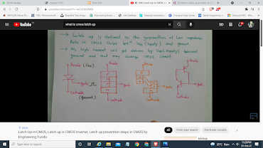
- let us take four-layer SCR like below and apply Vdd at the anode and GND at the cathode.
- after you are given the Vdd and GND, if we give a trigger( small pulse) at the gate the SCR will Turn ON now current flows through it but there is no chance to turn it Off, This is called latch-up in SCR.
- The above scenario is the same in the transistor topology of SCR.
- By redrawing the Mos circuit using Transistors we get:
- We can observe that the circuit we just drawn is the same as the circuit of SCR using transistors.
- There are two conditions in which the LATCH-UP happens they are:
- 1. if Vout > Vdd: in this case, the emitter of Q1 is high so as a result, the emitter-base junction gets forward biased, the output of Q1 drives current through Q2 so, Q2 also becomes forward biased.The current flows from Vdd to GND.
- 2. if Vout < GND: in this case the emitter-base junction of Q2 makes current driving into Q1 making Q1 also ON. This makes a path between Vdd and GND.
- By adding Gold impurities the lifetime of minority charge carriers increases by this we can minimize the latch-up.
- By adding an Epitaxial layer at the substrate.
- Place substrate and well as close as possible.
- Avoid forward Biased of Source and Drain.
- PMOS close to Vdd and NMOS close to GND.


Comments
Post a Comment